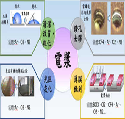
Plasma Applications
Cleaning Modification Roughening
Plasma surface treatment improves wire bonding strength and reduces the possibility of circuit failures. If residual photoresist, resin, solution residues and other organic contaminants are exposed on the product surface or interface gaps, they can be quickly removed using a plasma cleaning machine.
Drilling and De-smearing
During mechanical drilling or laser drilling of PCBs, high-temperature melting occurs and forms smear, which adheres to the inner copper edges and hole wall areas, causing poor contact during subsequent copper plating. Therefore, de-smearing must be performed before copper plating.
Photoresist Ashing
Plasma ashing process has good decomposition effects on hydrocarbons. The main application of ashing is the complete removal of photoresist layers during etching processes.
Thin Film Etching
Plasma etching can effectively remove surface defects and form smooth surfaces.

